
China Chips Face Cost Hurdles Without EUV
Chinese manufacturers are using older equipment to produce advanced processors, but the method increases production expenses and reduces output efficiency.
By Enzo Conti ·
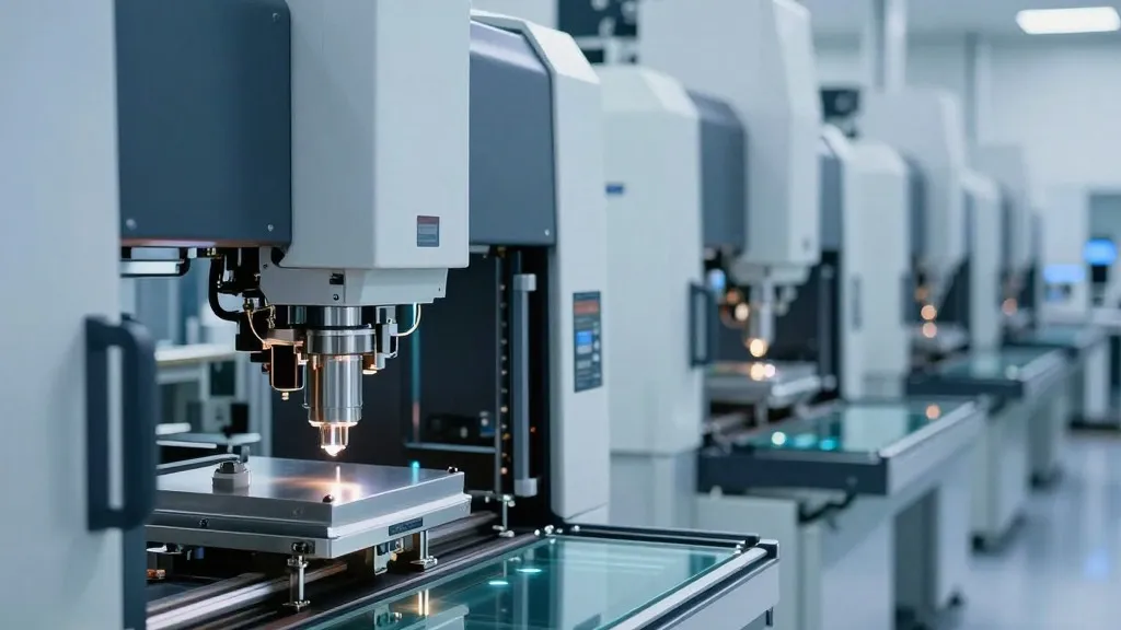
Export restrictions have blocked the most advanced lithography tools from entering China, forcing local chipmakers to rely on older deep ultraviolet equipment. This workaround allows for continued production of capable silicon, yet it introduces significant financial and technical hurdles for the industry.
The primary challenge lies in the method of multiple patterning. Instead of printing complex chip layers in a single pass, manufacturers using deep ultraviolet tools must split designs into several simpler patterns. Each additional exposure step increases the risk of defects and extends production timelines. Experts note that this approach creates a steep cost curve that makes advanced manufacturing less economical.
Chris Mack, co-founder and CTO of Fractilia, highlighted the trade-offs involved in bypassing extreme ultraviolet technology. He explained that industry standards suggest three exposures on older 193 immersion tools cost roughly the same as one advanced extreme ultraviolet exposure. However, when manufacturers require four masks to complete a layer, the advanced technology becomes the cheaper option. This economic shift places a heavy burden on companies trying to compete without the newest machinery.
Quality control presents another significant obstacle. Every new pattern must align perfectly with previous etched layers, and more exposures lead to accumulated errors. Designers often add extra space around features to compensate for these variations. This adjustment enlarges the chip size and reduces the number of usable dies per wafer. Since wafers cost tens of thousands of dollars, losing potential dies represents a substantial financial loss. Mack noted that businesses sell the final chips, not the raw wafers, making efficiency critical.
Memory chip production offers clear evidence of this efficiency gap. A June report from Morgan Stanley estimated that Chinese maker CXMT produces only about one-third as many bits per wafer as Western competitors. The bank described lithography access as a hard ceiling for development in this sector. While some node labels like 5nm have limited meaning in isolation, the physical differences in density and yield remain significant hurdles for Chinese firms.
Despite these constraints, older technology still has potential for further advancement. Micron previously developed its 1-alpha DRAM without using extreme ultraviolet light, relying instead on multiple patterning and tight process control. Mack stated that this approach pushed the limits of 193 immersion technology further than other memory makers. Analysts believe that CXMT can achieve similar goals for its planned HBM3e products, and advanced packaging techniques may extend the viability of this method through the end of the decade.
The outlook suggests a mixed future for Chinese chip manufacturing. Companies can continue to push older equipment by accepting larger die sizes, lower yields, or longer manufacturing times. Morgan Stanley projects that CXMT will increase its share of global DRAM supply from 14% in 2026 to 16% in 2028 through new capacity. The bank also expects China’s AI chip self-sufficiency to rise from 42% in 2025 to 70% by 2030, though gaps in advanced software and specific components will persist.
Source: Tom's Hardware